How Large Amounts of Data Fit Inside Tiny Storage Devices
Learn how microSD cards, SSDs and flash drives store huge amounts of data using microscopic memory cells, electrical charge and 3D NAND technology.

A microSD card measures only about 15 × 11 × 1 millimetres, yet modern flash storage can pack astonishing amounts of information into spaces this small. The SD standard itself now defines capacity classes extending far beyond the gigabyte range, even though the maximum allowed by a standard shouldn't be confused with the capacity of products currently available.
That raises an obvious question: where does all that data physically go?
A photo looks like a photo to us. A movie may contain billions of pixels and audio samples. A game can contain detailed 3D models, textures, music and millions of lines of code. But a storage chip doesn't store any of those things in the form we recognize.
At its lowest level, everything becomes bits: 1s and 0s.
The remarkable part isn't merely that computers represent information using bits. It is that semiconductor engineers have learned to manufacture billions upon billions of microscopic storage locations, distinguish extremely small differences in electrical state, place several bits inside each memory cell, and then stack those cells vertically in many layers.
The result is something that would once have required racks of storage hardware fitting into a device you can balance on a fingertip.
First, What Does "Storing Data" Actually Mean?
Consider a digital photograph.
The file contains numbers representing information such as pixel colours, image dimensions and other data needed to reconstruct the picture. Those numbers ultimately become binary information.
Text works the same way. So do videos, songs, applications and documents.
At the storage-hardware level, there is no tiny photograph or miniature movie hidden inside the chip. There are only physical states that electronics can interpret as data.
For a simple conceptual example:
01001101is eight bits.
A storage device needs some physical way to preserve those bits even after the power is removed.
Hard disk drives do this using magnetic states on rotating platters. Optical discs use physical or optical differences on a disc.
Most modern memory cards, USB flash drives, smartphone storage and SSDs instead rely primarily on NAND flash memory.
Unlike RAM, NAND flash is non-volatile, which means it can retain stored information without continuously receiving power.
Inside Flash Memory Is a Huge Grid of Tiny Cells
The fundamental storage elements inside NAND flash are called memory cells.
You can think of a cell as a microscopic electronic structure whose electrical characteristics can be changed deliberately and later measured.
A simplified NAND flash cell is built around a transistor. Depending on the NAND design, electrical charge can be stored in structures such as a floating gate or a charge-trap layer.
That stored charge changes a property called the transistor's threshold voltage: roughly speaking, how much voltage is required before the transistor begins conducting.
The chip's circuitry can measure that behaviour.
So instead of thinking:
"This cell contains a 1."
it is more accurate to think:
"This cell has been programmed into an electrical state that the memory circuitry interprets as a particular bit pattern."
That distinction becomes especially important because modern NAND cells often store more than one bit each.
One Cell No Longer Has to Mean One Bit
The simplest form of NAND is known as SLC, or Single-Level Cell.
An SLC cell stores one bit, which means it only needs to distinguish two logical states.
For example:
State A → 0
State B → 1
If you can reliably distinguish more electrical levels, however, one physical cell can represent more information.
With four possible states, a cell can encode two bits:
00
01
10
11
This is the basic idea behind MLC, which stores two bits per cell.
Increase the number of distinguishable states again and capacity rises further.
| NAND type | Bits stored per cell | Electrical states required |
|---|---|---|
| SLC | 1 | 2 |
| MLC | 2 | 4 |
| TLC | 3 | 8 |
| QLC | 4 | 16 |
That means a QLC cell doesn't simply answer a yes-or-no electrical question. The controller has to determine which of 16 possible ranges the cell's threshold voltage represents.
This is one of the major tricks behind high-capacity storage: engineers didn't just make more cells. They learned to make each cell encode more information.
But More Bits per Cell Come With a Trade-Off
Imagine trying to measure water in a container.
If you only need to distinguish between "empty" and "full," you have plenty of margin for error.
Now imagine dividing the same range into 16 carefully separated levels.
The measurement has to be much more precise.
Something similar happens in NAND flash. As more bits are stored in each cell, the electrical ranges representing different states sit closer together. That makes programming and reading the cell more demanding.
Higher-bit-per-cell NAND can therefore involve trade-offs in areas such as write endurance, programming behaviour, latency and error-correction requirements. Manufacturers compensate with sophisticated controllers, coding techniques and flash-management algorithms.
High density isn't free. It is an engineering balance.
Making Cells Smaller Was Only Part of the Story
For many years, one of the most obvious ways to increase semiconductor capacity was to make components smaller.
If each memory cell occupies less surface area, more cells can fit on the same silicon die.
Early generations of NAND therefore became denser partly through increasingly fine semiconductor manufacturing.
But shrinking cells indefinitely creates difficulties. When neighbouring cells become extremely close, electrical interference, charge behaviour and reliability become harder to control.
Eventually, NAND manufacturers increasingly adopted a different strategy:
Instead of only making the city denser, they started building skyscrapers.
The Big Breakthrough: 3D NAND
Traditional planar, or 2D NAND, arranged memory cells largely across the surface of a silicon die.
Modern 3D NAND adds another dimension.
Memory cells are built in vertical stacks, with many layers positioned above one another.
Imagine a large piece of land.
If you build only single-storey houses, the number of homes is constrained by the land available.
You could make every house smaller, but eventually that becomes impractical.
A tower solves the problem differently. The same footprint can accommodate far more rooms by adding floors.
3D NAND follows a broadly similar principle.
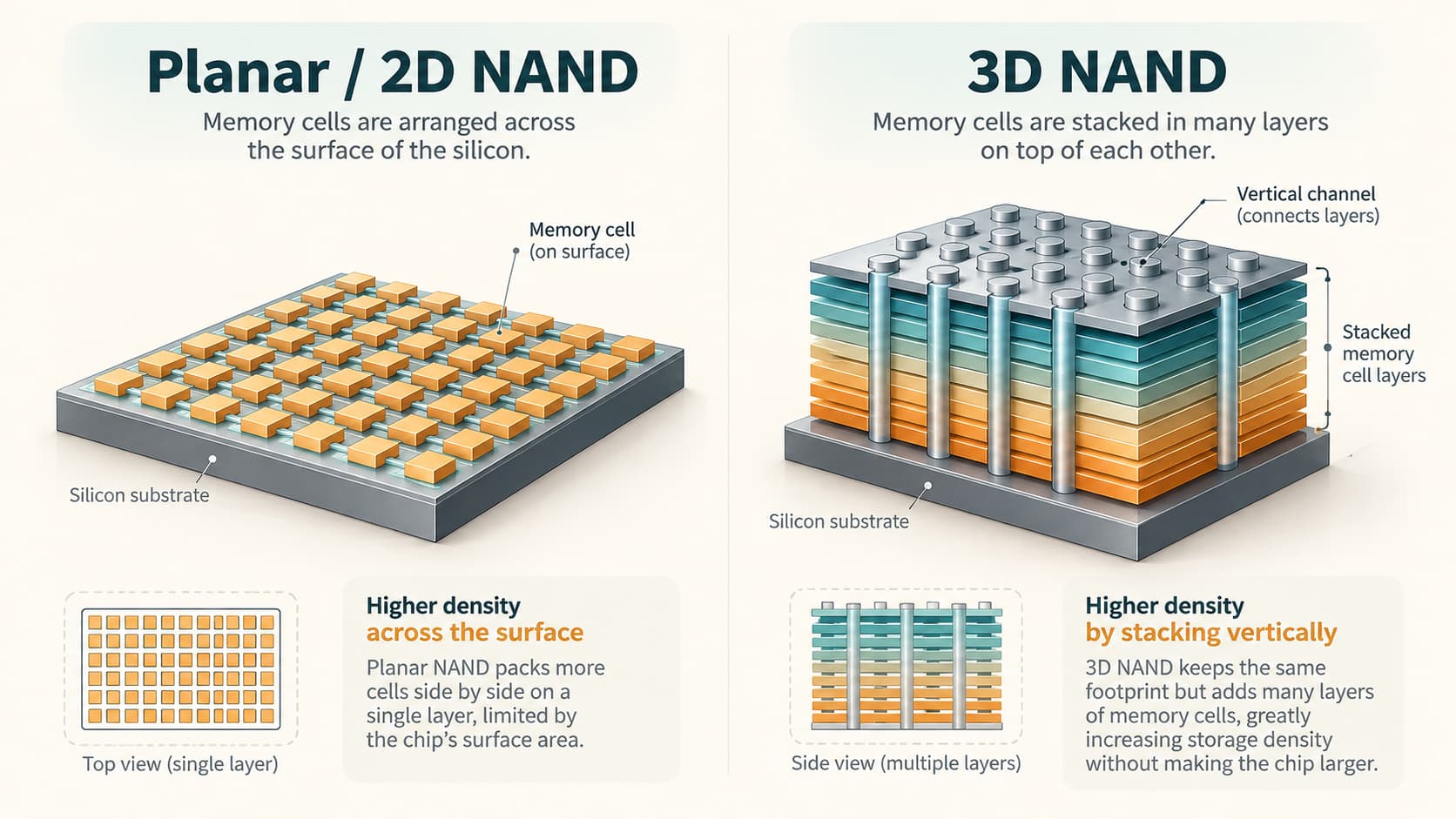
Instead of relying entirely on ever-smaller cells across a flat plane, manufacturers can increase density by adding more vertical memory layers and improving the structure of those layers.
Current commercial NAND has already moved into the hundreds of vertical levels.
This matters because adding more vertical layers allows manufacturers to increase the number of memory cells without relying only on shrinking their horizontal dimensions.
Chips Can Be Stacked and Packaged Too
The density story doesn't end inside an individual NAND die.
A storage product can combine multiple semiconductor dies inside a package, and a device may use several packages.
So there are several levels of density working together:
- Microscopic memory cells are manufactured extremely close together.
- Multiple bits can be encoded in one cell.
- Memory cells are stacked vertically using 3D NAND.
- Multiple NAND dies can be combined inside semiconductor packages.
- Multiple packages can be used within a complete SSD or other storage device.
The result is density on top of density.
This helps explain why a slim SSD can hold terabytes and why a tiny memory card can carry an amount of information that would once have required much larger storage systems.
Where Is the Controller in All of This?
A storage device isn't just a passive box full of memory cells.
It also needs intelligence to manage them.
Flash devices generally use a controller, a specialized processor that sits between the computer or phone and the raw NAND memory.
When your computer asks to save a file, the operating system thinks in terms of logical storage locations. It doesn't normally decide which exact physical NAND cell should receive each piece of data.
The controller handles much of that work.
Depending on the device, its responsibilities can include:
- translating logical addresses into physical flash locations
- detecting and correcting certain data errors
- managing worn or defective blocks
- distributing writes across the flash
- moving valid data during flash housekeeping
- managing spare storage areas
- optimizing performance
This management layer is essential because NAND flash has some unusual physical characteristics.
Flash Memory Cannot Simply Overwrite Data Wherever It Wants
From the user's perspective, changing a file seems simple.
Open document. Edit sentence. Press Save.
NAND flash has to do considerably more behind the scenes.
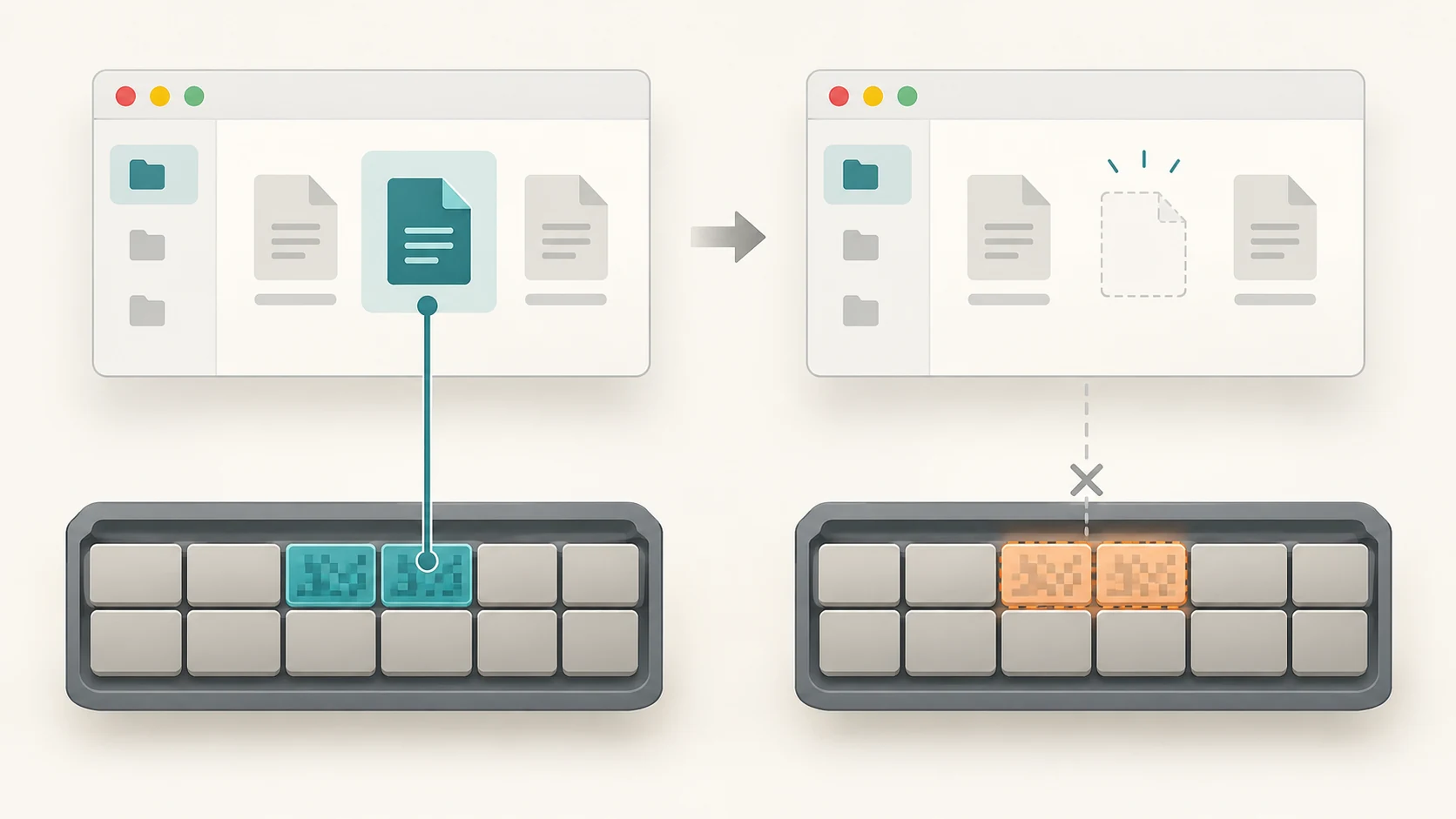
Flash memory is organized into structures commonly called pages and blocks.
Pages can be read and programmed, but erasing happens at the larger block level. A page containing old data cannot simply be overwritten indefinitely as though it were a character on a whiteboard.
Instead, the controller may need to write updated data elsewhere and eventually consolidate valid data so that old blocks can be erased and reused.
This process contributes to what is commonly called garbage collection.
Flash cells also tolerate a finite number of program/erase cycles. Controllers therefore use wear levelling to avoid repeatedly wearing out the same physical regions while other cells remain comparatively unused.
None of this increases the raw number of bits that physically fit in the NAND cells. But it is what allows incredibly dense flash memory to behave like a practical, reliable storage device.
How Can Such Tiny Electrical States Be Reliable?
At this scale, you might reasonably wonder how the device can distinguish all those closely spaced charge states without constantly corrupting files.
The answer is that modern flash storage assumes that raw NAND isn't perfect.
Controllers use error-correction codes, usually abbreviated ECC, which add redundant information that can help detect and correct certain errors when stored data is read.
Modern controllers may also use techniques such as:
- read retry
- bad-block management
- data refresh
- spare blocks
- wear levelling
- sophisticated signal-processing and error-correction algorithms
This is an important part of the answer to our original question.
Tiny storage isn't possible simply because engineers can manufacture microscopic cells. It works because the device also has mechanisms for managing the imperfections that appear when enormous numbers of those cells are packed together.
Is the Data Being Compressed to Make It Fit?
Sometimes files are compressed, but compression is not the main reason a 1 TB device can store 1 TB of data.
A JPEG photograph, MP3 audio file, ZIP archive or compressed video format may already use mathematical techniques to reduce the number of bits required to represent its content.
But storage capacity itself refers to how much digital information the device is designed to hold.
Put 100 GB of already-compressed video onto a flash drive and it still occupies roughly 100 GB of logical storage. The flash drive doesn't secretly turn every file into something dramatically smaller just to make its advertised capacity possible.
The extraordinary density comes mainly from the physical storage technology itself: extremely small cells, multiple bits per cell, three-dimensional structures and advanced packaging.
Compression is a separate layer.
Does a 1 TB Drive Actually Contain One Trillion Tiny Switches?
Not quite.
This is another reason the technology is more interesting than the simple "one transistor equals one bit" explanation.
With SLC NAND, one cell represents one bit.
With TLC, each cell represents three bits.
With QLC, each cell represents four.
And the flash device also contains capacity used for management, error correction, bad-block replacement and other internal purposes. The host computer sees a logical storage system rather than a direct one-to-one view of every physical NAND cell.
Modern storage is therefore not simply a giant row of microscopic on/off switches.
It is a carefully managed system in which analogue electrical behaviour is interpreted as digital information.
Why Can't Manufacturers Keep Increasing Capacity Forever?
Because every method of increasing density becomes more difficult as it is pushed further.
Adding more bits per cell requires distinguishing increasingly narrow voltage ranges.
Adding more 3D NAND layers makes fabrication more complicated. Manufacturers must create extremely deep, narrow structures through large stacks of material while keeping billions of cells uniform enough to work reliably.
Shrinking dimensions introduces additional electrical and manufacturing challenges.
More density can also create trade-offs involving:
- endurance
- write performance
- error rates
- manufacturing complexity
- power consumption
- heat
- cost
That is why storage development isn't simply a race to make every component smaller.
Engineers continually balance capacity, speed, reliability, endurance and manufacturing cost.
The Tiny Card Is Really a Microscopic Machine
Pick up a microSD card and it appears almost disappointingly simple: a piece of plastic, a few electrical contacts and some printed markings.
Internally, however, it represents several layers of extraordinary engineering.
Your photograph is converted into bits.
Those bits become patterns represented by electrical states inside NAND cells.
Each cell may represent several bits by using multiple carefully controlled threshold-voltage ranges.
Huge numbers of those cells are manufactured in microscopic structures.
The structures are stacked vertically into 3D NAND.
Multiple dies can be assembled into compact packages.
A controller continuously translates addresses, corrects errors, manages wear and hides much of the physical complexity from your phone or computer.
And all of this happens inside something small enough to lose between the cushions of a sofa.
That is the real explanation for how enormous amounts of data fit into tiny storage devices. The data itself hasn't somehow become physically smaller. Semiconductor engineering has simply become extraordinarily good at representing more information in less material and less space.